Nanotechnology - Atomic Force Microscope
Broad Air Review on atomic force microscopes for MSE 505
Authors
Shawn Le Cody Baxter Brandon Touchet
Abstract
Abstract - The Atomic Force Microscope, or AFM, is examined relative to its usefulness in characterizing and quantifying of biological systems. An introduction to its operation and use in these systems is given. The AFM is then discussed based on various biological applications. Biological applications are given emphasis and include DNA imaging, relative imaging time, living cells, biosensors, biofilms, and tissue scaffolds. The material is then summarized. Carbon nanotube research has been rapidly expanding and progressing rapidly for the past decade. With advances in technology, novel solutions to ineffectively treated problems and devices are constantly being proposed. In addition, many previously used medical procedures have been improved with the newly exploited carbon structures. Carbon nanotubes are proving to be more beneficial than initially proposed. This paper is intended to provide a general understanding of carbon nanotubes and a basic understanding of their role in photothermal therapy. Dip Pen Nanolithography (DPN) is a versatile tool that utilizes the AFM to write ink into nanopatterns on a substrate. Because of the AFM tip ability to attract different material of ink, it can be used in many applications such as biology, chemistry, and semiconductor. The applications are abundant and can help advance nanotech devices. This paper reviews the DPN process and its recent advances in research to increase its throughput and applications.
Introduction
The atomic force microscope (AFM) is an imaging tool that is used to generate high resolution images of nonconductive hard or soft surfaces. The capability of the AFM to provide high-resolution images of nonconductive soft surfaces makes it a great tool for imaging a range of biological samples [1, 2]. Biomolecules ranging in size from DNA to blood cells can be imaged with the AFM because of this capability. Because it can operate in liquid environments and there is no special coating of the sample necessary, biological studies under physiological conditions are possible. This is very unlike samples and working environments for other methods such as the scanning electron microscope or the tunneling electron microscope, even though they provide images of similar resolution as the AFM [2].
Similarly, in contrast to other imaging methods, biological samples can be prepared in such a way that their molecular dynamics can be viewed with the AFM for long periods of time while still in a natural state without damage [3]. And, the AFM has extremely high spatial resolution that allows users to study individual biological molecules such as proteins and the relationships of their molecular dynamics and functions relative to their structures and functionalities. While the AFMs have the capability of distinguishing single atoms in hard materials, it can still be used to image soft biological specimens providing the applied force of the stylus is very low so as to prevent structural damage to the softer biological samples [3].
In 1999 DPN was demonstrated by using the AFM to transfer simple organic molecules to the surfaces [4]. About 20 years ago, IBM demonstrated nanomanipulation by moving individual xenon atom on a nickel substrate to form an IBM logo[4].
AFM Setup
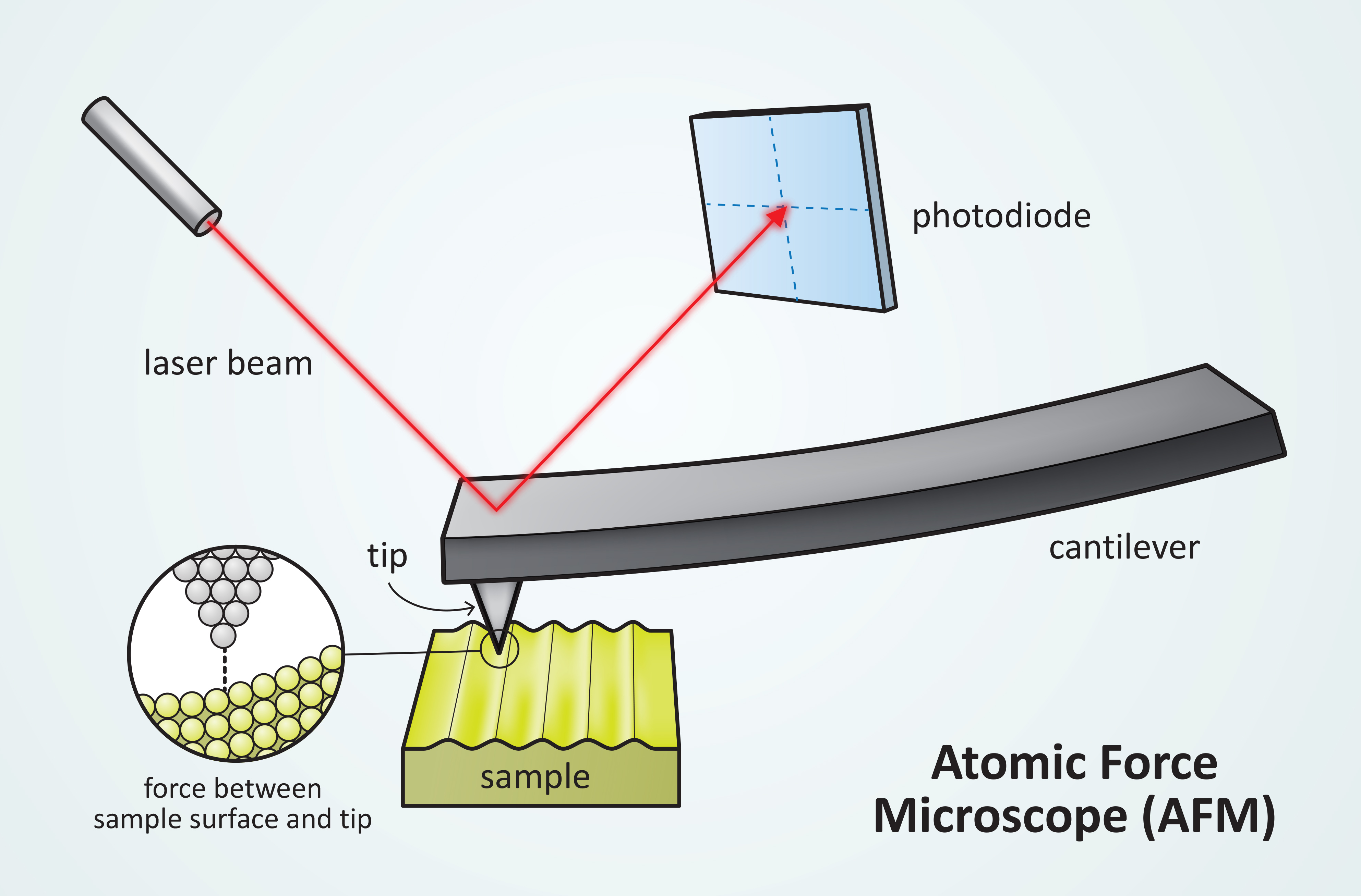
The AFM cantilever interacts by the repulsive or attractive force between the probe tip and sample surface which causes the cantilever to deflect up and down. There is a distance for this attractive and repulsive force as shown in Figure 2. The deflection of the cantilever is measured with a laser pointed on the top of the cantilever and the laser is reflected back to a photodetector for measurement as shown in Figure 1.
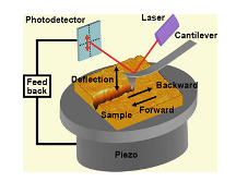 Figure 1. A diagram of the cantilever deflection from scratching a surface. The laser is reflected to a photodetector to measure the deflection. The sample is on a piezo table with feedback control to adjust the interaction distance between the tip and sample [4].
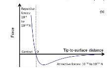 Figure 2: The repulsive force and attractive interaction as a function of distance between the probe tip and sample surface.
There are two methods of measurement with the AFM, contact-mode and dynamic-mode. The contact-mode operates within the repulsive interactive force of the tip and sample. The tip is dragged along the sample surface causing the cantilever to deflect from changes in the surface topography. The dragging causes wearing of the tip and can produce degradation of the sample. Therefore, contact-mode is not suitable for certain applications [5].
The dynamic-mode operates through cantilever oscillations. An external stimulus such as piezo material attached to the cantilever induces oscillations in cantilever. The probe interacts with the sample between the attractive and repulsive force. This method is gentler on the sample and is preferred for soft and biological samples.
Biological Applications
DNA Imaging
The AFM has been modified to operate under cryogenic temperatures and under very low vacuum for viewing DNA plasmids under contact mode [1]. However, when viewing high-resolution images of wet biological molecules, it must be kept in mind that it is easy to deform these molecules from the force applied to the AFM tip. Heat also induces motion in the samples causing difficulties in obtaining a sharp image, which can be counteracted by operating the AFM at low temperatures.
Cryogenic AFM operation and subsequent sample temperature lowering increases mechanical stability in DNA macromolecules and virtually eliminates any thermally induced effects. The cantilever tip is also less subject to thermal effects and so less noise is seen from the instrument itself. However, this means that the sample is no longer in a physiological state, much like with electron microscopes.
Operating the AFM at liquid nitrogen temperature is suitable for DNA and most other proteins because they freeze and become hard and rigid when cooled to below 180 K [1].
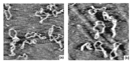 Figure 3: DNA plasmids under (a) ambient conditions and (b) cryogenic temperatures [1].
Imaging Time
The imaging speed of the AFM has been of concern in much of the recent research when imaging biological specimens [2,3,6]. Short time ranges are required to capture clear topographs of moving specimens [3].
Typically when trying to image a specific biological sample or molecule such as chromosomes, AFMs must make multiple scans of large surfaces because these objects are randomly distributed on the substrate [2]. And, so, most of the time spent imaging is devoted to locating the object and not to producing an image of the object itself. To rectify this, an AFM can be integrated with EPI illumination from an inverted optical microscope. This modified AFM can image objects 1pm or larger. Specimens of interest can be quickly selected by moving the entire sample with an XY stage. An image is then taken with the optical microscope and then is either reflected or fluoresced. This image can then be compared to the image taken by the AFM based on the amount of overlap in the fields of view [2].
Faster imaging times are necessary to obtain real-time images of dynamic biological processes, including mineral dissolution and growth and polymer crystallization, and work is being done in probe sensitivity enhancement and faster in and out of plane speeds of the scanner [6].
Living Cells
Cells must be kept alive when they are viewed interacting with stimuli [7]. Cells are typically just a few micrometers in size, and proteins, in tens of angstroms, are even smaller. The study of living cells and their interactions with their external environment is crucial when developing medications. Other essential factors include cell adhesion and growth characteristics. Nanoparticles and nanostructures can be used for cell or molecule modification and drug delivery without causing great damage to the cells or molecules themselves because of their relative sizes.
Traditionally, the optical microscope has been used to view cells, but since live cells have very low contrast and their internal structures are virtually colorless, they must be stained and fixated to a slide or subjected to other processes that kill them before they can be viewed. The optical microscope, like any other imaging method, has its limitations. For example, the image must be dark or highly refractive. Resolution is limited to about 0.2 microns by diffraction and unfocused light from surrounding sources distort the image. Electron microscopes overcome most of the limits of the optical microscope, but the cells lives are still compromised during sample preparation.
Biological cells are soft and do not adhere well to substrate surfaces unlike hard material samples. This makes imagining of such materials much more difficult with the AFM. Nonetheless, the AFM has an advantage over the other imaging methods. The AFM is capable of imaging micron-sized objects such as biological cells in a wet environment; thus, cell life and integrity is not so easily compromised [7].
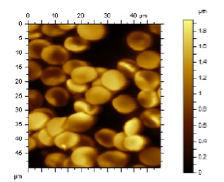 Figure 4: AFM image of red blood cells in blood plasma on glass slide [7].
Biofilms
Pilli, flagella, polysaccharides, proteins, and most other nanostructures found in biofilms are in the extracellular matrix and range from 50-150 nm in width and 1-10 nm in thickness [8]. These nanostructures have a direct influence on bacterial biofilm stability based on their spatial arrangement. For example, this arrangement and biofilm stability is important in dealing with wastewater treatment, biofiltration, and biocide enhancement. This presents a need for enhanced imaging methods with resolution on the nanoscale.
Standard analysis of biofilms and biopolymers is done using confocal laser scanning microscopy, or CLSM. Like other traditional methods for viewing biological molecules, CLSM requires staining and spatial resolution is limited. CLSM alone cannot determine the arrangement and distribution of nanostructures in the matrix of biofilms and biopolymers. However, the CLSM can be combined with the AFM. Imaging of such small molecules is possible with the AFM and the images show the heterogeneous composition of biofilms in a nanometer scale. Combining these two provides excellent nanoscale resolution of CLS micrographs and it is therefore easy to identify and quantify nanostructures and their interactions within the biofilms.
Further combination of the CLSM-AFM system with Raman spectroscopy provides further enhancement. If a metal or metal-coated tip is used with the AFM the laser focus improves the signals from the Raman spectroscope and a fingerprint of spectra can be obtained allowing better quantification of sample composition [8].
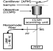 Figure 5: AFM combined with CLSM [8]
Biosensors
Many applications require the need for highly advanced sensitive biosensors [9]. The major problem with their design is that of the interaction of the bio-interface with the transducer surface. Nanopatterned surfaces offer a solution to this disadvantage because they can be used as an interface between the incompatible biological sample and the transducer surface.
Diagnosis of diseases can be time consuming and early stage detection is not always possible. Especially when dealing with critical diseases, high performance and high sensitivity biosensors could satisfy the need for early disease screening, detection, and diagnosis. Their development and ability to define diseases in their early stages would be an asset to the current healthcare system and would reduce the need for therapy and cost of care while simultaneously giving a more positive outlook to the patient.
Other applications for biosensors are the food industry and rapid detection of biological pathogens and bioterrorism agents [9].
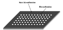 Figure 6: Nanopatterned surface with bioadhesive for use in AFM [9]
Rissue Scaffolds
Hard material implants in biological systems suffer from host tissue detachment, bioincompatibility, low adhesion, and can result in cell integration [10]. Recent efforts towards tissue engineering to solve these problems have gained favor with current medical research. Tissue engineering in this area involves finding suitable alternatives for replacing the non-compatible hard material implants by using more compatible biological materials. Reduced need for repeated operations to replace implants, rejection of implants by body tissues, disease transmission, and even donated organ rejection is feasible. This research starts with the need for biodegradable tissue scaffolds on which cells can be adhered, or seeded. Requirements for the scaffolds are that they must be biocompatible, biodegradable, and provide a reliable structure for the cells to seed. The AFM provides an excellent method to study the surface morphology of these scaffolds and biocompatible implants as it can image in wet environments. And so, the biological environment that these scaffolds and tissues are found in naturally can be imitated in the AFM [10].
Lipid Bilayers
In addition to topographical properties, the AFM can readily be used to examine biomechanical properties. Recent interest has been in using planar supported lipid bilayers (SLB) as model systems [11]. Either single or multiple-layered lipids can be used, and can be prepared using vesicle fusion, Langmuir-Blodgett or Langmuir-Schaefer deposition. Bilayered lipids are the most common because the majority of lipid layers in biological systems are found in the cell membrane. AFMs can then be used to study these by first scanning the probe tip across the unaltered lipid bilayer.
Information is then recorded on lateral domain extent and surface roughness and heights of patches. Then, a surface molecule, or, effector molecule, is attached to the lipid bilayer and the topography is reexamined. Typically, hydrocarbons, antibiotics, peptides, and other drugs serve as the effector molecules. Taking these topographical images of the surface before and after the effector molecule is attached gives information about time dependent interactions of the effector molecule with the lipid bilayer.
Another approach of evaluating the biomechanical changes done by the effector molecule is by bringing the probe tip toward the bilayer while constantly increasing the load of the tip until the layer ruptures and the supporting substrate is sensed. This process is repeated several times. Force-distance approach curves are generated, and any discontinuities corresponding to rupture events are analyzed and associated force magnitudes are determined and averaged to provide an identifying fingerprint of the bilayer [11].
It should also be noted that biological molecules can be attached to the tip itself and similar analyses can be performed [12].
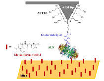 Figure 7: Biologically altered AFM tip
Relative Humidity
When selecting materials and conditions for packaging and storing of biological molecules, it is important to understand the effects of relative humidity on adhesive forces between the biological molecules and their polymer substrates [6]. The AFM can be used to study these capillary forces. These forces, when measured by the AFM, are influenced by factors similar to those associated with pull-off forces in dry conditions.
The liquid bridge that is formed when these forces are measured at a high relative humidity is affected by the substrate surface roughness, particle shape, and particle size. The AFM tip composition itself also affects the liquid bridge and the critical pull-off force [12].
DPN Deposition
Introduction
DPN is a novel method for fabricating nanostructures that employ the atomic force microscope (AFM). This process is essential to nanotechnology as it is proven to be a versatile tool to alternative lithographic system such as the electron beam, ion beam, and X-ray lithography [2]. These alternative processes require a vacuum and cannot operate under ambient conditions like the DPN process. The DPN process builds nanostructures in single step pattern, allowing freedom in size, shape, and position [4].
For a simplistic comparison, DPN is similar to a quill pen feather dipped in ink solution then used to write on a surface substrate with the combined precision and resolution of an AFM. DPN is essentially an AFM cantilever with the probe tip coated with material such as gold to electrically or chemically attract molecules (ink) and the ink are then transfer to a substrate by means of diffusion. When the coated tip is brought close to the ink, molecules from the ink are attracted to the tip. The molecules on the tip are then deposited onto the strip by forming a liquid meniscus between the tip and the substrate as shown in Figure 8. The meniscus is important for the transfer of the ink to the substrate because this allows the diffusion of particles from the tip to the substrate. The diffusion phenomena in a meniscus was studied in [5], by creating a meniscus in a two phase liquid and oil, and was observed to gain better understanding of the meniscus diffusion transport phenomena. Humidity, distance between tip and substrate, tip radius, temperature, and ink properties are parameters that determine the resolution and how the meniscus form [13].
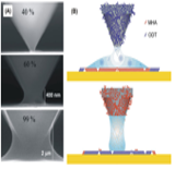 Figure 8: SEM images of meniscus formed between the tip and substrate in (A). In top (B) shows image of hydrophilic and in bottom (B) shows image of hydrophobic meniscus [4].
DPN has several advantages that make it an attractive process. The environmental condition can affect the resolution and line width of the deposited structure, but what makes it more appealing is that it can be performed in ambient conditions. This can be advacntageous for patterning of biological materials such as proteins, nucleic acids, viruses, and cells [14]. DPN does not require resist material and masking like other nanolithographic processes, making it more suitable for rapid prototyping. Two disadvantages that DPN presents are the slow rate of nanopatterning and the patterning area limitation. The area is limited to about 100 mm x 100 mm [14]. However, the writing process could be increased with an array of cantilevers that pattern in parallel. However, the cantilever array and writing of the array convolutes the process.
A multiple cantilevers fabrication process will develop variations in parameters such as the spring constants [14], requiring maintenance of feedback controls for each individual cantilever. Cantilever dimensions and stage surface variations would require extra effort to align each cantilever, in the array, to the substrate. Therefore, DPN array is an important configuration that will be surveyed in this paper. One of the attributes to DPN versatility is the ability to deposit diverse form of nanoparticles in nanometer resolution. The following will review the deposit technique and review some recent applications for some of the methods. The first method is the conventional method that commonly used organic molecules such as a thiol group linker attached to long-chain hydrocarbons as ink to transport the ink from the tip of the AFM to a gold surface [4, 15]. The second method is an additive enhanced deposition method that used additives to affect the diffusion of the ink in the meniscus. One example is a surfactant added to the ink to increase its wettability resulting in increase of ink transfer [4]. A third deposition method requires a voltage to increase the driving force and control the deposition by switching on or off. Some nanoparticle materials that have been implemented with include: polymers, fullerenes, gold nanoparticles [4,16]. A fourth deposition method is temperature-assisted deposition. Increases in temperature, accelerates the deposition rate and allows for on and off control. One application of this deposition method is the use of Indium metal [17], discussed later
After the ink deposition step, there are different chemical reactions that take place in the meniscus to pattern the desired material on the substrate. These reactions are electrochemical reduction, hydrolysis reaction, etching reaction, and others [4].
DPN Applications
Arranging the cantilever tip in array increasesarray increases the throughput of the DPN process. As mentioned earlier, there are mechanical variationare mechanical variations for each individual probe when fabricated. So there is a need to individually control each cantilever in the array when pattering the substrate. Actuation of each cantilever tip is an important characteristic of the array arrangement and the following present recent research in actuation of cantilever array.
One form of actuation is thermal DPN (tDPN) [818] which allows for the ability to turn “on” or “off” deposition of the ink because certain inks are solid in room temperature [818]. One approach usesd a resistor integrated into the cantilever to allow ing for melting of the ink and deposit material such as metal [717]. Nelson, and et al,. demonstrated the first metal deposition in a continuous layer with Indium, shown in Fig. 3. Nelson They proved that tDPN can overcome the limitation of deposition of DPN with metal.
This work provides potential applications in the electronic industry. Futuremore, nanocircuits and nanowires can be directly written and fabricated for use. However, Indium has a low melting point of 156.6 °C, high wettability surfaces, and the electrical resistivity of deposited indium oxide varies from 1010^4-10^8-4 to108 Ω-cm depending on deposition conditions [717]. There is still a need for deposition of other metal type with low resistivity to build future potential nanocircuits. One other challenge for other metal deposition with tDPNn is the high melting point that is required to deposit the metal ink. Other metal deposition would make DPN more attractive to nanocircuit patterning. Lastly, tDPN of metal is still needed to be integrated as an array for future production scale.
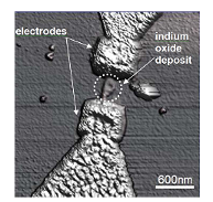 Figure 9: AFM image of tDPN of indium oxide between two gold electrodes.
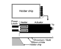 Figure 9: AFM image of tDPN of indium oxide between two gold electrodes.
Thermal actuation is not only used at the tip but is also used to deflect the cantilever probes as shown in Fig. 4 to write pattern in an array of cantilevers [8]. Most DPN cantilever array write in the same pattern (not individually controlled), whereas in [13], [18] report of active probes that are arranged in array and controlled independently from other probe in the array. These cantilevers are usually made of silicon nitride and an additional layer of gold is added to create a bimorph actuator [18]. Bullen and et al. demonstrated DPN with thermal actuation in an array to increase throughput. The thermal actuation heat source from the resistive layer could potential conduct to the ink and have a negative effect on its deposition. This was not mentioned by Bullen and et al. The conducted heat on the tip could have an effect on the meniscus and result in undesirable width pattern and further study should be conducted.
Another method of ink deposition from tip to substrate is through electrostatic force. In Lim’s study, electrostatic interaction is used to pattern nanoscale conducting polymer on a modified silicon substrate as shown in Figure 11 [16]. Polymers such as self-doped sulfonated polyaniline (SPAN) and doped polypyrrole (PPy) are charged and can be deposited on a charged silicon surface. However, the silicon substrate needs to be modified (functionalized) to either positive or negative charged to attract the opposite charged polymer. One drawback Lim had was the inability to deposit polymer on unmodified silicon surfaces. Therefore, this technique is still limited but it can lead to potential application in electrical, optical, and sensing devices that consist of conductive polymer. Conductive polymers have its potential in screens and light emitting diode. DPN used for conductive polymer is a promising tool for prototyping and build nanostructure of these electrical devices. Using DPN for production scale is still far reached due to its limitation with throughput even with high density probe array.
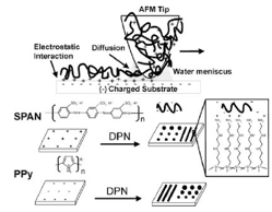 Figure 11: DPN of conductive polymer on a substrate through electrostatic interactions between modified charged substrate and opposite charged polymer. [16]
Others report study of using DPN to write organic patterns. DPN can be used to make functional devices that utilize organic materials. One study used hexamethyldisilazane (HMDS) as ink that can write feature less than 100 nm line width onto Si/SiOx and oxidized GaAs [15].
In addition to functionalized polymer in [16], for biological application, the substrate surface are functionalized to attached biological molecules for sensing specific molecules and viruses. DPN was used to functionalized different DNA sequence on a gap between two electrodes in different junctions on a chip shown in Fig. 6 [19] for sensing. The ability to be able to functionalized different chemicals and molecules on chip could potentially lead to more versatile chip that can sense more than one type of bacteria, viruses, and diseases on a single chip. DPN may help make the leap for biosensor to sense multiple diseases.
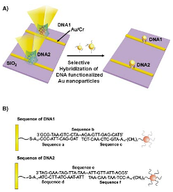 Figure 12: (a) show the functionalize surface and Au nanoparticles deposited on an Au/Cr substrate. (a) show the how schematic of the functionalized DNA Au nanoparticle attached to the functionalized surfaced.
One of the weaknesses of DPN is the need to refill the tip with ink from depletion of writing on the structure. A novel method to overcome this is continuous feed of the ink from a reservoir shown[20], [21] as can be seen in Figure 13. The capillary force in the small microchannel feed the ink to the tip of the cantilever without the aid of a pump which makes this an attractive design. With this design, Kim patterned monolayers of alkanethiol on to gold and later study show patterning with other inorganic and biomolecules. Kim did not mention if the patterning of the inorganics and biomolecules required gold substrate or other less expensive materials. Furthermore, Kim tested the fountain-pen DPN nanolithography in array to expand its capabilities as shown in Figure 14.
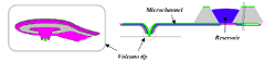 Figure 13: Nano-fountain probe. A volcano shape tip (left) and a reservoir with microchannel that feed ink to the tip for continuous writing [21].
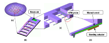 Figure 14: (a) Show the concept of the fountain pen cantilever in parallel. (b) and (c) show a close up view of microfluidic channel and a bending actuation underneath to control tip vertical motion [20].
Carbon Nanotube Tips
Background
Carbon Nanotubes (CNTs) are monatomic or poly-atomic layers of graphite. A single layer of graphite is known as graphene. Graphene can be stacked three layers thick before it loses its unique thermal and electronic properties. After three layers, graphene tends to behave more like graphite. On the most basic level, the monatomic layers of graphene are geometrically repeated, six hexagonally-bonded carbon atoms. The nature of the covalently bonded carbon is what provides the resilience of this unique material [22].
CNTs can be manufactured as single-walled CNTs (SWCNT) or multiwalled CNT (MWCNT), concentric single-walled CNTs. SWCNTs generally have a diameter of of 0.4-2 nm, while MWCNTs tend to have a diameters of 2-100 nm. With a length to diameter ratio can be as large as 10^4-10^5 [22]. By definition MWCNTs have at the least two layers of graphene layers, but may have as many as thirty concentric layers [23].
Properties
TThere are three basic types of CNTs: armchair, zigzag, and chiral. In chemistry the term chirality refers to molecules without mirror symmetry. Thus, it follows that chiral CNTs do not have mirror symmetry, while armchair and zigzag have mirror symmetry. The three different types of CNTs can be formed by rolling a piece of graphene in one of three different directions defined by two basis vectors, a_1 & a_2, and their respective coefficients, n& mϵZ^+ ^+ [1324]. An example of a chiral type characteristic vector can be seen in Figure 1, where n=5 & m=2.
Armchair nanotubes’ characteristic folding vector is defined by C ⃗=na_1+ma_2, where n=m. By rolling a graphene sheet along (C ) ⃗an armchair nanotube is formed. To form a zigzag nanotube, roll the graphene sheet along C ⃗=na_1, where m=0. Finally, when m≠n the characteristic vector, C ⃗=na_1+ma_2, defines the chiral type. Figure 2 depicts the three types of nanotubes.
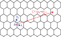 Figure 15: Representation of the basis vectors and the chiral type (n=5 & m=2) [25]
The three types of CNTs can be subdivided into metallic and non-metallic or semiconducting. Using the basis vector coefficients, if n-m=3k , where k=0,1,2,3,… the CNT is metallic [1526]. All other CNTs are classified as semi-conducting. Metallic or conducting CNTs have over lapping conduction and valence bands. It is the overlap that allows easy transport of electrons, which gives metals their intrinsic electrical properties. Semi-conductors have small gaps between their conduction and valence bands. Electrons in the semi-conductor’s valence band need an energy boost greater than the energy gap between the top of the conduction band and the bottom of the conduction band for the material to act as a conductor. Without the extra energy, the semi-conductor should act like an insulator, with small probability of electron tunneling.
Bunder and Hill show that the rule mentioned above is an approximation for CNTs with very small radii and no applied strain [1627]. Their model is founded on the premise that a real lattice is better defined as one which has irregularly shaped hexagons with three distinct bond lengths [1627].
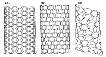 Figure 16: (a) zigzag, (b) chiral, and (c) armchair [28]
Deriving energies from the more realistic model allows for more adequate application of nanotubes. Dresselhaus, et al, supports Bunder and Hill by stating, “for most experimentally observed carbon nanotube sizes, the gap in the tiny-gap variety, which arises from curvature effects, is so small that, for most practical purposes, all the n-m=3k tubes can be considered as metallic at room temperature” [1829]. On the atomic scale small fluctuations become significant changes. It is also the electronic band structures that allows for photothermal therapy [19]. Therefore, more attention should be attributed to realistic modeling of CNTs to allow for more appropriate and accurate applications.
The importance of understanding the different electronic properties can bring new novel electronic devices by combining two or more types of CNTs [1829]. With proper CNT combinations or strategically applying defects, CNTs can form metal-semiconductor, semiconductor-semiconductor, or metal-metal junctions [1829]. The combination of different structures alters the band gaps. One result of altering band gaps is the production of a nanodiode by combining a metal and semiconducting nanotube [1829].
Tip Modification
The AFM tip is an important aspect of the AFM. As nano research demand for nanoscale resolution measurement, conventional silicon tip cannot achieve such task. Recent synthesis of silicon nanowire (SiNW) and carbon nanotube (CNT) tip on the AFM cantilever is promising for nanoscale resolution and high aspect ratio surface feature. Chikamoto and et al. reported the synthesis of single-walled carbon nanotubes (SW-CNTs) bundled on the tip of the AFM by dielectrophoresis (DEP) technique. Chikamoto mentioned other methods of growing CNTs on the AFM tip through chemical vapor deposition (CVD) and manual attachment. The DEP method can be performed at room temperature and pressure and is low cost giving it advantage over the CVD method. An AC electric is generated between a tungsten probe and the cantilever tip and the CNT bundle is synthesize as the probe pulls away. The DEP-CNT tip based AFM provide better resolution compared to usual AFM and even other commercial cantilever and good wear resistance. High step aspect ratio step structures were also practical due to the high aspect ratio of the CNT [21].
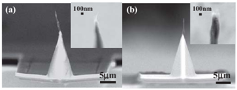 Figure 17: SEM image of the SW-CNT on the AFM tip [21].
Engstrom, et al, reported a new technique for synthesis of multiwalled carbon nanotube tips (MWNT) and silicon nanowire (SiNW) tip can that be fabricated using aligned wafer scale nanostencil lithography. The nanostencil mask is used to deposit the catalyst material for the growth. The MWNTs are grown using plasma enhanced chemical deposition (PECVD) and the SiNW are grown by the vapor-liquid-solid method as shown in Figure 18. SiNW are cylindrical and the tip of a cylinder structure wear have less image broadening compared to worn sharp tips. MWNT lateral stiffness is greater than SWNT and is preferable for high aspect ratio metrology [22]. MWNTs are also grown with CVD, however it have defects that lessened their lateral stiffness and can buckle [22].
 Figure 18: SiNWs grown in Fig. 10c and MWNTs grown as shown in Fig. 10d. Fig. 10a and b show the nanostencil lithography method [22].
Conclusions
Since the AFM is an excellent tool for interatomic force studies, and lends itself well to topographical imaging of both hard and soft samples, both in ambient conditions and under liquids, it lends itself well to imaging of biological species. It is able examine a greater variety of surface interactions and develop mathematical models for similar inorganic, organic, and biological systems than other conventional techniques, especially the traditional optical light microscope.
While a robust tool for generating high resolution images of smooth surfaces on a nanometer level, the atomic force microscope, or AFM, is limited. The AFM tip range of measurement and the tip-sample interaction result in strong nonlinearities in tip motion, inaccuracies in measurements, and detrimental wear of the tip occur. Its simplicity and especially resolution does allow it to be used for viewing unmodified biological samples in a natural environment and in special cases of modified environments. This review paper has shown DPN to be useful in biological, electrical, and chemical applications due to its versatility to build biosensors, chemical sensors, and electrical circuits. Some of the paper reviewed here has shown to overcome some of DPN drawbacks. Parallel array cantilever increases the surface deposition rate and increase the patterning throughput. Each probe in the array is controlled by actuation to compensate for misalignment and give it freedom for patterning. Not addressed in this paper is how the individual control of high density array can lead to complex computer computations and mundane tuning of individual cantilever. More control system research of cantilever probes can address individual tuning of probes. One technique comes to mind is adaptive tuning technique in control system that can be implemented. The disadvantage of having to constantly dip the tip in ink was overcame with the advance of continuous ink feed from a reservoir. Continuous ink feed will be useful for future commercialization of DPN.
Different ink applications and materials were discussed in this review. Polymer, metals, DNA, organics, and inorganics, are just some of the inks that could be used. Although the drawback for some surface needed to be functionalized to accept nanoparticles such as DNA, DPN can expand the versatility of biosensor by allowing more than one functionalized molecules in the chip sensor.
The future research of DPN should be to increase its role not only in research prototyping, but application in commercial production of micro and nanodevices.
The AFM is an excellent tool for interatomic force studies, and lends itself well to topographical imaging of both hard and soft samples, both in ambient conditions and under liquids. Coating the tip with various molecules, inorganic, organic, and biological, allow the user to examine a greater variety of surface interactions and develop mathematical models for similar inorganic, organic, and biological systems.
While a robust tool for generating high resolution images of smooth surfaces on a nanometer level, the atomic force microscope, or AFM, is limited. The AFM tip range of measurement and the tip-sample interaction result in strong nonlinearities in tip motion, inaccuracies in measurements, and detrimental wear of the tip occur. Its simplicity does allow it to be used for viewing unmodified surfaces in a natural environment and in special cases of modified environments.
References
[1] A. Radenovic, et al. “A low-termperature ultrahigh vacuum atomic force microscope for biological applications,” Rev. Sci. Instrum., vol. 74, no. 2, pp. 1022-1026, Feb. 2003.
[2] C. A. J. Putman, et al. “Atomic force microscope with integrated optical microscope for biological applications,” Rev. Sci. Instrum., vol. 63, no. 3, pp. 1914-1917, Mar. 1992.
[3] D. J. Muller, et al. “Folding, Structure and Function of Biological Nanomachines Examined by AFM,” AIP Conf. Proc., vol. 696, no. 1, pp. 158-165, 2003.
[4] A. A. Tseng, Ed., Tip-Based Nanofabrication Fundamentals and Applications. New York: Springer, 2011.
[5] K. Salaita, et al, “Sub-100 nm, centimeter-scale, parallel dip-pen nanolithography.,” Small (Weinheim an der Bergstrasse, Germany), vol. 1, no. 10, pp. 940–5, Oct. 2005.
[6] I. S. Bozchalooi, et. al., “Compensator design for improved counterbalancing in high speed atomic force microscopy,” Rev. Sci. Instrum., vol. 82, no. 11, pp. 113712-1 – 113712-12, Nov. 2011.
[7] D. Chicea, et. al., “The Application of AFM for Biological Samples Imaging,” Dig. J. Nanomater. Bios., vol. 5, no. 4, pp. 1015-1022, Oct. 2012.
[8] T. Schmid, et. al., “Towards chemical analysis of nanostructures in bofilms I: imaging of biological nanostructures,” Anal. Boanal. Chem., vol. 391, no. 5, pp. 1899-1905, Jul. 2008.
[9] P. Lisboa, et. al., “Nanopatterned Surfaces for Bio-Detection,” Anal. Lett., vol. 43, no. 10/11, pp. 1556-1571, Jul. 2010.
[10] G. A. Abdel Hakeam, et. al., “Laser Surface Modification of Poly (-caprolactone) Scaffold for Artificial Skin Applications,” Am. J. Biomed. Sci., vol. 5, no. 1, pp. 1-13, Sept. 2012.
[11] S. J. Attwood, et. al., “Preparation of DOPC and DPPC Supported Planar Lipid Bilayers for Atomic Force Microscopy and Atomic Force Spectroscopy,” Int. J. Mol. Sci., vol. 14, pp. 3514-3539, Feb. 2013.
[12] A. C. N. da Silva, et. al., “Nanobiosensors Based on Chemically Modified AFM Probes: A Useful Tool for Metsulfuron-Methyl Detection,” Sensors, vol. 13, pp. 1477-1489, Jan. 2013.
[13] M. Zhang, et al. A. Mirkin, “Passive and Active Probe Arrays for Dip-Pen Nanolithography,” IEEE-NANO, vol. S1.2 Nanol, pp. 27–31, 2001.
[14] K. Salaita, et al. “Sub-100 nm, centimeter-scale, parallel dip-pen nanolithography.,” Small (Weinheim an der Bergstrasse, Germany), vol. 1, no. 10, pp. 940–5, Oct. 2005.
[15] A. Ivanisevic and C. A. Mirkin, “‘Dip-Pen’ nanolithography on semiconductor surfaces.,” Journal of the American Chemical Society, vol. 123, no. 32, pp. 7887–9, Aug. 2001.
[16] B. J. Lim and C. A. Mirkin, “Electrostatically Driven Dip-Pen Nanolithography,” Advanced Materials, vol. 14, no. 20, pp. 1474–1477, 2010.
[17] B. A. Nelson, et al, “Direct deposition of continuous metal nanostructures by thermal dip-pen nanolithography,” Applied Physics Letters, vol. 88, no. 3, p. 033104, 2006.
[18] D. Bullen, et al. In, D. Pen, and N. Dpn, “Design , Fabrication , and Characterization of Thermally Actuated Probe Arrays for Dip Pen Nanolithography,” Journal of Microelectromechanical Systems, vol. 13, no. 4, pp. 594–602, 2004.
[19] S.-W. Chung, et al, “Top-down meets bottom-up: dip-pen nanolithography and DNA-directed assembly of nanoscale electrical circuits.,” Small (Weinheim an der Bergstrasse, Germany), vol. 1, no. 1, pp. 64–9, Jan. 2005.
[20] K. Kim, et al, “Massively parallel multi-tip nanoscale writer with fluidic capabilities—fountain pen nanolithography (FPN),” in 4th International Symposium on MEMS and Nanotechnology, 2003, vol. 60208, no. d, pp. 235–238.
[21] K. Kim, et al, “A Novel AFM Chip for Fountain Pen Nanolithography - Design and Microfabrication,” in Material Research Society Symposium Proceedings, 2004, vol. 782, pp. 1–6.
[22] R. Saito, et al. ”Structure of a Single-Wall Carbon Nanotube” in Physical Properties of Carbon Nanotubes, World Scientific Publishing Co., 1998, ch. 3, sec. 3.1-3.2, pp. 35-39.
[23] S. Sarojini, et, al. ” CARBON NANOTUBES: A NEW WEAPON IN HEALTH CARE TREATMENT,” Int. J. of Pharma and Bio Sciences, vol. 1, no. 4, pp. 644-649,Oct.-Dec. 2010.
[24] R. Saito, et al. ”Structure of a Single-Wall Carbon Nanotube” in Physical Properties of Carbon Nanotubes, World Scientific Publishing Co., 1998, ch. 3, sec. 3.1, pp. 37.
[25] Kato Group, Institute of Engineering Innovation, School of Engineering, The University of Tokyo. (2012 Apr. 3) Chirality of single-walled carbon nanotubes [Online]. Available: http://ykkato.t.utokyo.ac.jp/Nanotubeschiralty.en.html
[26] A. A. Adams. (2000). Physical Properties of Carbon Nanotubes [Online] Available: http://www.pa.msu.edu/cmp/csc/ntproperties/
[27] J. E. Bunder and J. M. Hill. ”Electronic properties of carbon nanotubes with distinct bond lengths,” J. of Appl. Phys., vol. 107, no. 2 2010.
[28] D. T. Baviskar, ”Carbon Nanotubes: An Emerging Drug Delivery Tool In Nanotechnology,” Int. J. of Pharmacy and Pharmaceutical Sciences, vol. 4, no. 4, pp.11-15, 2012
[29] M. S. Dresselhaus, et al. ”Electronic, thermal and mechanical properties of carbon nanotubes,” Philosph. Trans. of The Roy. Soc. A: Math., Physical, and Eng. Sci., vol. 362, no. 1823, pp. 2065-2098, 13 Aug. 2004.
[30] Z. Lui, et al. “Carbon Nanotubes in Biology and Medicine: In vitro and in vitro Detection, Imaging and Drug Delivery,” Nano research, vol. 2, no. 2, pp. 85-120. 2009.